 | –≠–ª–µ–∫—Ç—Ä–æ–Ω–Ω—ã–π –∫–æ–º–ø–æ–Ω–µ–Ω—Ç: CD74HC670 | –°–∫–∞—á–∞—Ç—å:  PDF PDF  ZIP ZIP |
1
Data sheet acquired from Harris Semiconductor
SCHS195
Features
∑ Simultaneous and Independent Read and Write
Operations
∑ Expandable to 512 Words of n-Bits
∑ Three-State Outputs
∑ Organized as 4 Words x 4 Bits Wide
∑ Buffered Inputs
∑ Typical Read Time = 16ns for CD74HC670 V
CC
= 5V, C
L
= 15pF, T
A
= 25
o
C
∑ Fanout (Over Temperature Range)
- Standard Outputs . . . . . . . . . . . . . . . 10 LSTTL Loads
- Bus Driver Outputs . . . . . . . . . . . . . 15 LSTTL Loads
∑ Wide Operating Temperature Range . . . -55
o
C to 125
o
C
∑ Balanced Propagation Delay and Transition Times
∑ Significant Power Reduction Compared to LSTTL
Logic ICs
∑ HC Types
- 2V to 6V Operation
- High Noise Immunity: N
IL
= 30%, N
IH
= 30% of V
CC
at V
CC
= 5V
∑ HCT Types
- 4.5V to 5.5V Operation
- Direct LSTTL Input Logic Compatibility,
V
IL
= 0.8V (Max), V
IH
= 2V (Min)
- CMOS Input Compatibility, I
l
1
µ
A at V
OL
, V
OH
Description
The Harris CD74HC670 and CD74HCT670 are 16-bit register
files organized as 4 words x 4 bits each. Read and write
address and enable inputs allow simultaneous writing into one
location while reading another. Four data inputs are provided
to store the 4-bit word. The write address inputs (WA0 and
WA1) determine the location of the stored word in the register.
When write enable (WE) is low the word is entered into the
address location and it remains transparent to the data. The
outputs will reflect the true form of the input data. When (WE)
is high data and address inputs are inhibited. Data acquisition
from the four registers is made possible by the read address
inputs (RA1 and RA0). The addressed word appears at the
output when the read enable (RE) is low. The output is in the
high impedance state when the (RE) is high. Outputs can be
tied together to increase the word capacity to 512 x 4 bits.
Pinout
CD74HC670, CD74HCT670
(PDIP, SOIC)
TOP VIEW
Ordering Information
14
15
16
9
13
12
11
10
1
2
3
4
5
7
6
8
D1
D2
D3
RA1
RA0
Q3
GND
Q2
V
CC
WA0
WA1
WE
RE
Q0
Q1
D0
January 1998
CAUTION: These devices are sensitive to electrostatic discharge. Users should follow proper IC Handling Procedures.
Copyright
©
Harris Corporation 1998
File Number
1660.1
CD74HC670,
CD74HCT670
High-Speed CMOS Logic
4x4 Register File
[ /Title
(CD74H
C670,
CD74H
CT670)
/Subject
(High-
Speed
CMOS
Logic
4x4 Reg-
ister
2
Functional Diagram
9
6
7
10
Q0
Q1
Q2
Q3
4
11
15
1
3
D0
D2
WE
RE
5
14
13
RA1
RA0
WA0
WA1
12
2
D1
D3
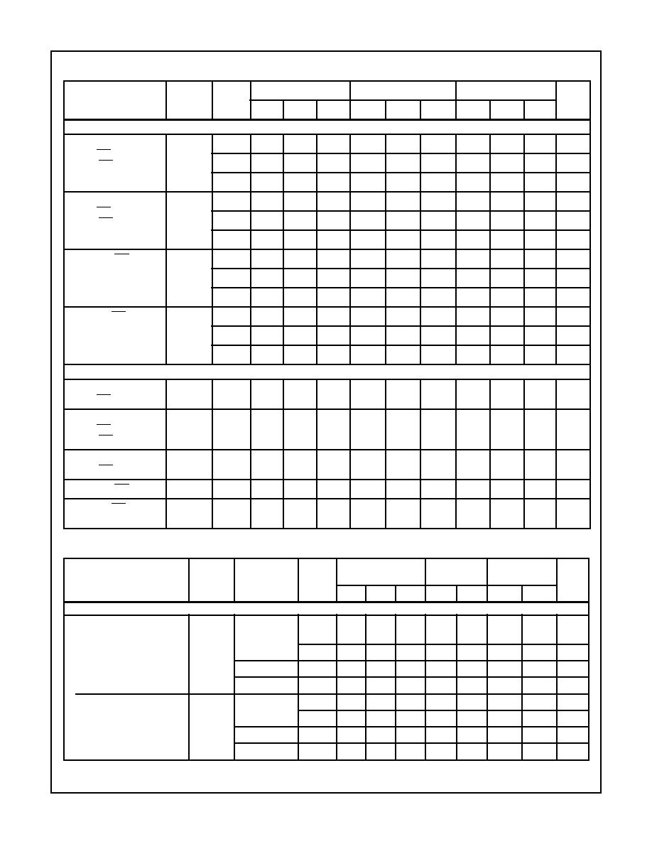
WRITE MODE SELECT TABLE
OPERATING
MODE
INPUTS
INTERNAL
LATCHES
(NOTE 3)
WE
D
N
Write Data
L
L
L
L
H
H
Data Latched
H
X
No Change
NOTE:
3. The Write Address (WA0 and WA1) to the "internal latches" must
be stable while WE is LOW for conventional operation.
READ MODE SELECT TABLE
OPERATING
MODE
INPUTS
OUTPUT
Q
N
RE
INTERNAL
LATCHES
(NOTE 4)
Read
L
L
L
L
H
H
Disabled
H
X
(Z)
NOTE:
4. The selection of the "internal latches" by Read Address (RA0 and
RA1) are not constrained by WE or RE operation.
H = High Voltage Level
L = Low Voltage Level
X= Don't Care
Z = High Impedance "Off" State
CD74HC670, CD74HCT670
CD74HC670, CD74HCT670
3
Absolute Maximum Ratings
Thermal Information
DC Supply Voltage, V
CC
. . . . . . . . . . . . . . . . . . . . . . . . -0.5V to 7V
DC Input Diode Current, I
IK
For V
I
< -0.5V or V
I
> V
CC
+ 0.5V
. . . . . . . . . . . . . . . . . . . . . .±
20mA
DC Output Diode Current, I
OK
For V
O
< -0.5V or V
O
> V
CC
+ 0.5V
. . . . . . . . . . . . . . . . . . . .±
20mA
DC Drain Current, per Output, I
O
For -0.5V < V
O
< V
CC
+ 0.5V
. . . . . . . . . . . . . . . . . . . . . . . . . .±
35mA
DC Output Source or Sink Current per Output Pin, I
O
For V
O
> -0.5V or V
O
< V
CC
+ 0.5V
. . . . . . . . . . . . . . . . . . . .±
25mA
DC V
CC
or Ground Current, I
CC
. . . . . . . . . . . . . . . . . . . . . . . . .±
50mA
Operating Conditions
Temperature Range, T
A
. . . . . . . . . . . . . . . . . . . . . . -55
o
C to 125
o
C
Supply Voltage Range, V
CC
HC Types . . . . . . . . . . . . . . . . . . . . . . . . . . . . . . . . . . . . .2V to 6V
HCT Types . . . . . . . . . . . . . . . . . . . . . . . . . . . . . . . . .4.5V to 5.5V
DC Input or Output Voltage, V
I
, V
O
. . . . . . . . . . . . . . . . . 0V to V
CC
Input Rise and Fall Time
2V . . . . . . . . . . . . . . . . . . . . . . . . . . . . . . . . . . . . . . 1000ns (Max)
4.5V. . . . . . . . . . . . . . . . . . . . . . . . . . . . . . . . . . . . . . 500ns (Max)
6V . . . . . . . . . . . . . . . . . . . . . . . . . . . . . . . . . . . . . . . 400ns (Max)
Thermal Resistance (Typical, Note 5)
JA
(
o
C/W)
PDIP Package . . . . . . . . . . . . . . . . . . . . . . . . . . . . .
90
SOIC Package . . . . . . . . . . . . . . . . . . . . . . . . . . . . .
160
Maximum Junction Temperature . . . . . . . . . . . . . . . . . . . . . . . 150
o
C
Maximum Storage Temperature Range . . . . . . . . . .-65
o
C to 150
o
C
Maximum Lead Temperature (Soldering 10s) . . . . . . . . . . . . . 300
o
C
(SOIC - Lead Tips Only)
CAUTION: Stresses above those listed in "Absolute Maximum Ratings" may cause permanent damage to the device. This is a stress only rating and operation
of the device at these or any other conditions above those indicated in the operational sections of this specification is not implied.
NOTE:
5.
JA
is measured with the component mounted on an evaluation PC board in free air.
DC Electrical Specifications
PARAMETER
SYMBOL
TEST
CONDITIONS
V
CC
(V)
25
o
C
-40
o
C TO 85
o
C -55
o
C TO 125
o
C
UNITS
V
I
(V)
I
O
(mA)
MIN
TYP
MAX
MIN
MAX
MIN
MAX
HC TYPES
High Level Input
Voltage
V
IH
-
-
2
1.5
-
-
1.5
-
1.5
-
V
4.5
3.15
-
-
3.15
-
3.15
-
V
6
4.2
-
-
4.2
-
4.2
-
V
Low Level Input
Voltage
V
IL
-
-
2
-
-
0.5
-
0.5
-
0.5
V
4.5
-
-
1.35
-
1.35
-
1.35
V
6
-
-
1.8
-
1.8
-
1.8
V
High Level Output
Voltage
CMOS Loads
V
OH
V
IH
or V
IL
-0.02
2
1.9
-
-
1.9
-
1.9
-
V
-0.02
4.5
4.4
-
-
4.4
-
4.4
-
V
-0.02
6
5.9
-
-
5.9
-
5.9
-
V
High Level Output
Voltage
TTL Loads
-
-
-
-
-
-
-
-
-
V
-6
4.5
3.98
-
-
3.84
-
3.7
-
V
-7.8
6
5.48
-
-
5.34
-
5.2
-
V
Low Level Output
Voltage
CMOS Loads
V
OL
V
IH
or V
IL
0.02
2
-
-
0.1
-
0.1
-
0.1
V
0.02
4.5
-
-
0.1
-
0.1
-
0.1
V
0.02
6
-
-
0.1
-
0.1
-
0.1
V
Low Level Output
Voltage
TTL Loads
-
-
-
-
-
-
-
-
-
V
6
4.5
-
-
0.26
-
0.33
-
0.4
V
7.8
6
-
-
0.26
-
0.33
-
0.4
V
Input Leakage
Current
I
I
V
CC
or
GND
-
6
-
-
±
0.1
-
±
1
-
±
1
µ
A
CD74HC670, CD74HCT670
CD74HC670, CD74HCT670
4
Quiescent Device
Current
I
CC
V
CC
or
GND
0
6
-
-
8
-
80
-
160
µ
A
Three- State Leakage
Current
V
IL
or V
IH
V
O
=
V
CC
or
GND
6
-
-
±
0.5
-
±
5.0
-
±
10
µ
A
HCT TYPES
High Level Input
Voltage
V
IH
-
-
4.5 to
5.5
2
-
-
2
-
2
-
V
Low Level Input
Voltage
V
IL
-
-
4.5 to
5.5
-
-
0.8
-
0.8
-
0.8
V
High Level Output
Voltage
CMOS Loads
V
OH
V
IH
or V
IL
-0.02
4.5
4.4
-
-
4.4
-
4.4
-
V
High Level Output
Voltage
TTL Loads
-6
4.5
3.98
-
-
3.84
-
3.7
-
V
Low Level Output
Voltage
CMOS Loads
V
OL
V
IH
or V
IL
0.02
4.5
-
-
0.1
-
0.1
-
0.1
V
Low Level Output
Voltage
TTL Loads
6
4.5
-
-
0.26
-
0.33
-
0.4
V
Input Leakage
Current
I
I
V
CC
and
GND
0
5.5
-
±
0.1
-
±
1
-
±
1
µ
A
Quiescent Device
Current
I
CC
V
CC
or
GND
0
5.5
-
-
8
-
80
-
160
µ
A
Three- State Leakage
Current
V
IL
or V
IH
V
O
=
V
CC
or
GND
5.5
-
-
±
0.5
-
±
5.0
-
±
10
µ
A
Additional Quiescent
Device Current Per
Input Pin: 1 Unit Load
I
CC
V
CC
-2.1
-
4.5 to
5.5
-
100
360
-
450
-
490
µ
A
NOTE: For dual-supply systems theoretical worst case (V
I
= 2.4V, V
CC
= 5.5V) specification is 1.8mA.
DC Electrical Specifications
(Continued)
PARAMETER
SYMBOL
TEST
CONDITIONS
V
CC
(V)
25
o
C
-40
o
C TO 85
o
C -55
o
C TO 125
o
C
UNITS
V
I
(V)
I
O
(mA)
MIN
TYP
MAX
MIN
MAX
MIN
MAX
HCT Input Loading Table
INPUT
UNIT LOADS
WE
0.3
WA0
0.2
WA1
0.4
RE
1.5
DATA
0.15
RA0
0.4
RA1
0.7
NOTE: Unit load is
I
CC
limit specific in DC Electrical Specifications
Table, e.g., 360
µ
A max. at 25
o
C.
CD74HC670, CD74HCT670
CD74HC670, CD74HCT670
5
Prerequisite for Switching Specifications
PARAMETER
SYMBOL
V
CC
(V)
25
o
C
-40
o
C TO 85
o
C
-55
o
C TO 125
o
C
UNITS
MIN
TYP
MAX
MIN
TYP
MAX
MIN
TYP
MAX
HC TYPES
Setup Time
Data to WE
Write to WE
t
SU
, t
h
2
60
-
-
75
-
-
90
-
-
ns
4.5
12
-
-
15
-
-
18
-
-
ns
6
10
-
-
13
-
-
15
-
-
ns
Hold Time
Data to WE
Write to WE
t
H
, t
W
2
5
-
-
5
-
-
5
-
-
ns
4.5
5
-
-
5
-
-
5
-
-
ns
6
5
-
-
5
-
-
5
-
-
ns
Pulse Width WE
t
W
2
80
-
-
100
-
-
120
-
-
ns
4.5
16
-
-
20
-
-
24
-
-
ns
6
14
-
-
17
-
-
20
-
-
ns
Latch Time WE to RA0,
RA1
t
LATCH
2
100
-
-
125
-
-
150
-
-
ns
4.5
20
-
-
25
-
-
30
-
-
ns
6
17
-
-
21
-
-
26
-
-
ns
HCT TYPES
Setup Time
Data to WE
t
SU
, t
h
4.5
12
-
-
15
-
-
18
-
-
ns
Hold Time
Data to WE
Write to WE
t
H
, t
W
4.5
5
-
-
5
-
-
5
-
-
ns
Setup Time
Write to WE
t
SU
4.5
18
-
-
23
-
-
27
-
-
ns
Pulse Width WE
t
W
4.5
20
-
-
25
-
-
30
-
-
ns
Latch Time WE to RA0,
RA1
t
LATCH
4.5
25
-
-
31
-
-
38
-
-
ns
Switching Specifications
C
L
= 50pF, Input t
r
, t
f
= 6ns
PARAMETER
SYMBOL
TEST
CONDITIONS
V
CC
(V)
25
o
C
-40
o
C TO
85
o
C
-55
o
C TO
125
o
C
UNITS
MIN
TYP
MAX
MIN
MAX
MIN
MAX
HC TYPES
Propagation Delay
t
PLH
, t
PHL
C
L
= 50pF
Reading Any Word
2
-
-
195
-
245
-
295
ns
4.5
-
-
39
-
49
-
59
ns
C
L
= 15pF
5
-
16
-
-
-
-
-
ns
C
L
= 50pF
6
-
-
33
-
42
-
50
ns
Write Enable to Output
t
PLH
, t
PHL
C
L
= 50pF
2
-
-
250
-
315
-
375
ns
4.5
-
-
50
-
63
-
75
ns
C
L
= 15pF
5
-
21
-
-
-
-
-
ns
C
L
= 50pF
6
-
-
43
-
54
-
64
ns
CD74HC670, CD74HCT670
CD74HC670, CD74HCT670